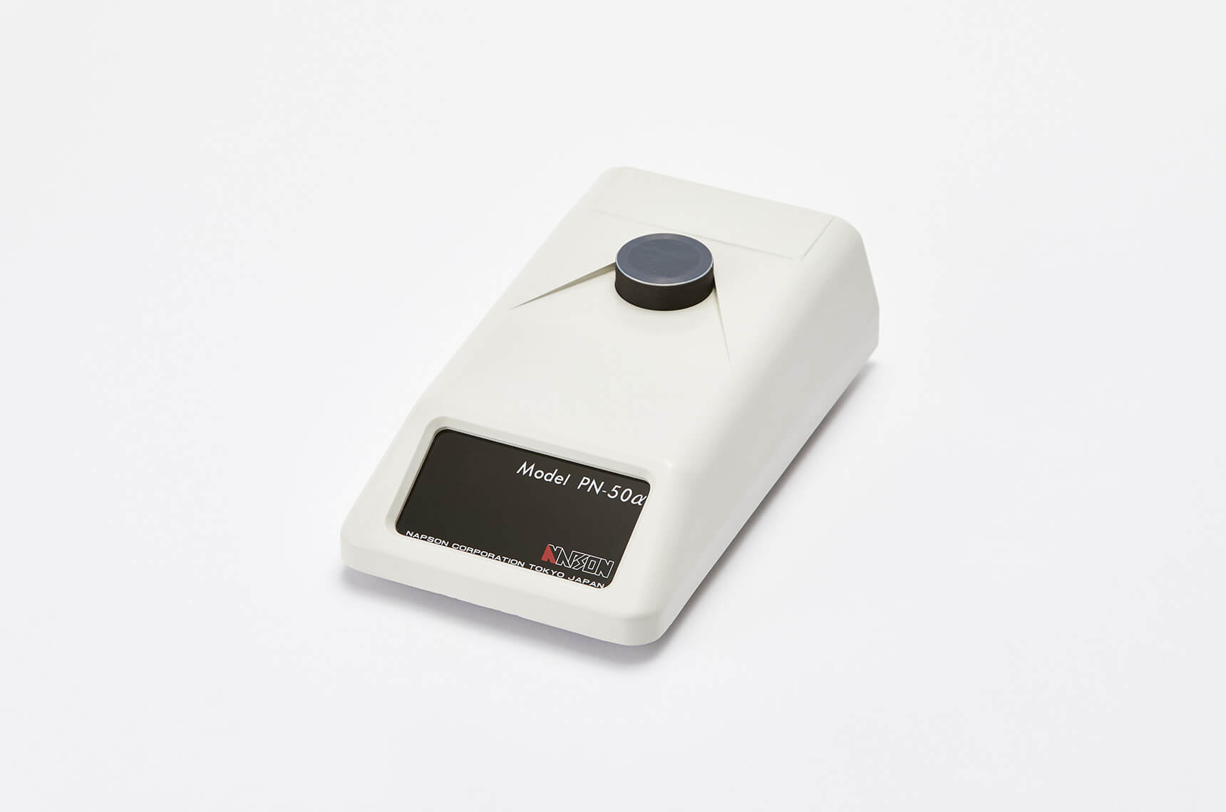
- Principle : Photovoltaic effect by light pulse irradiation - No damage and no stain by Non-contact method
- Possible to check even oxidized film on wafer surface
- Instantly discrimination by optical pulse illuminate
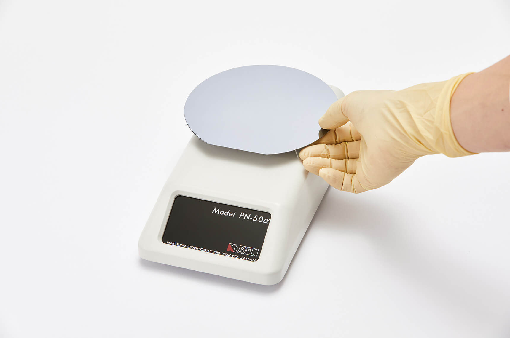
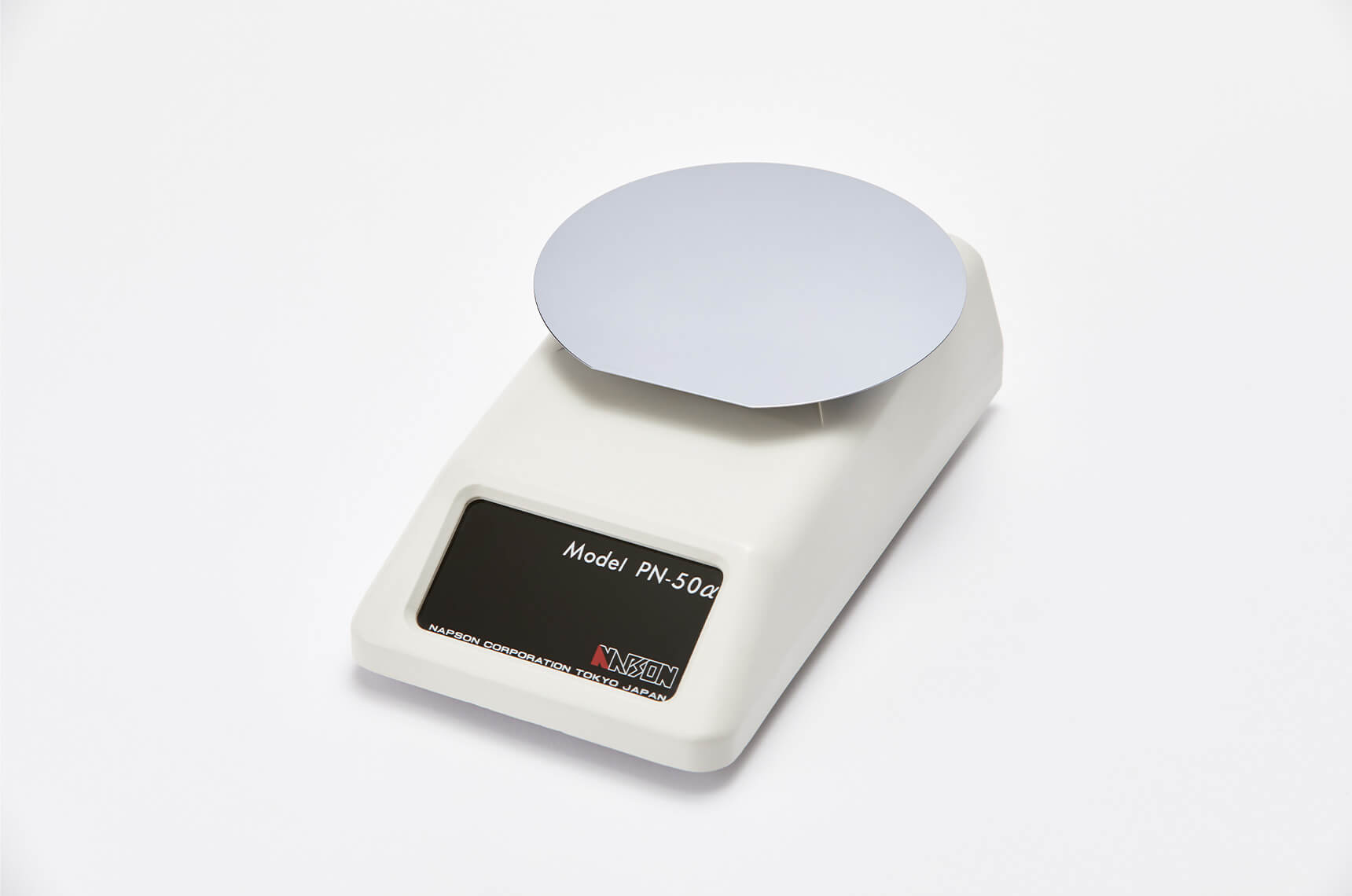
Applications - Semiconductor materials, Solar-cell materials (Silicon, Polysilicon)
Sample size - more than 30 x 30mm
Measuring range - PN Checking range in resistivity : 0.1 ~ 1,000 ohm-cm
|


 PN판정기
PN판정기 제품별 > PN판정기