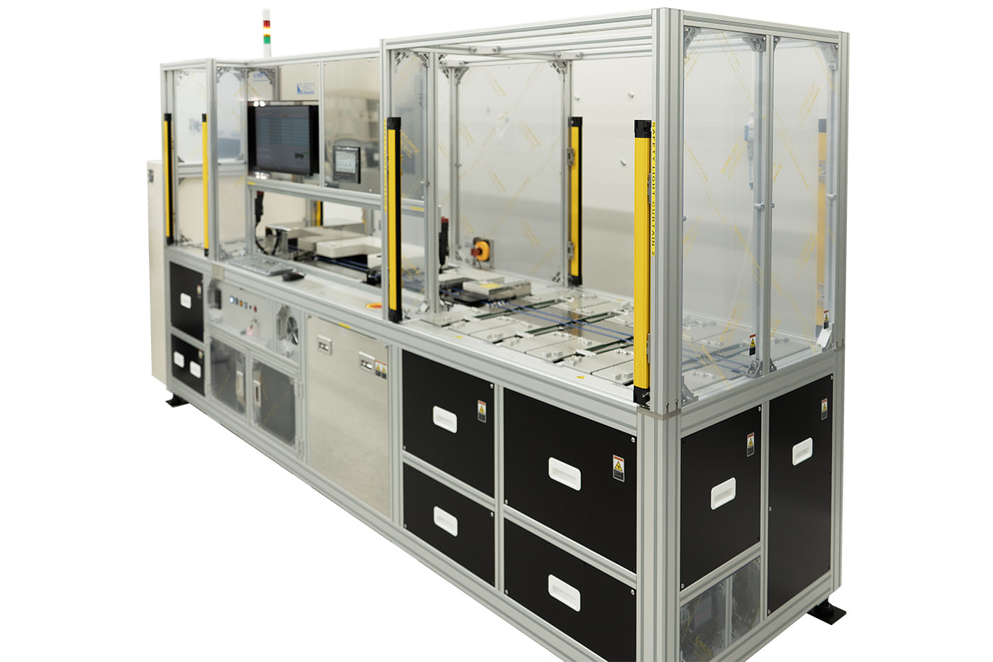
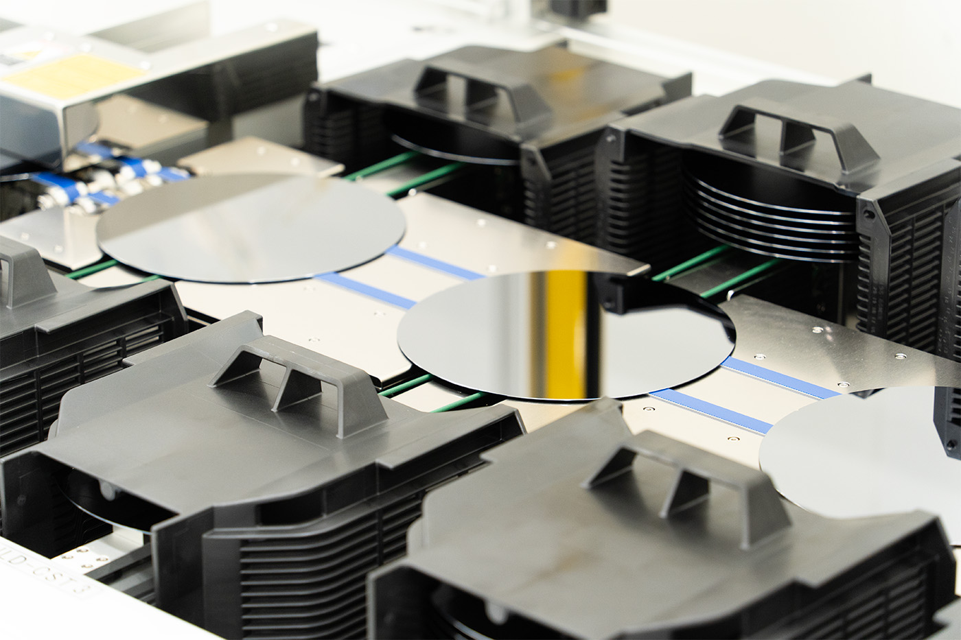
- Non contact measurement of resistivity, thickness and conductivity (P/N) - Number of cassette station can be changed by customers request - Eddy current method for resistivity, Electric capacitance method for wafer thickness - Temperature correction for silicon wafer function
Applications
- Semiconductor materials, Solar-cell materials (Silicon, Polysilicon, SiC etc)
Sample sizes
- 3~8 inch
Measuring range
- [R] 1m~200 ohm-cm - [Thickness] 150~800μm (300μm between 150 and 800μm is recommended) * The range is separated from each Low, Middle, High and Super High probe type.
* Please refer the measurement range for each probe type as below
(1) Low : 0.1~0.5 ohm/sq (0.001~0.05 ohm-cm) (2) Middle : 0.5~10 ohm/sq (0.05~0.5 ohm-cm) (3) High : 10~1000 ohm/sq (0.5~60 ohm-cm) (4) S-High : 1000~3000 ohm/sq (60~200 ohm-cm)
Video
|


 비접촉식 면저항측정기
 제품별 > 비접촉식 면저항측정기