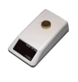
- Principle : Photovoltaic effect by light pulse irradiation - No damage and no stain by Non-contact method - Possible to check even oxidized film on wafer surface - Instantly discrimination by optical pulse illuminate


 제조사별
제조사별 제조사별
제조사별