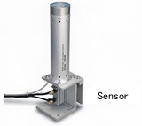
- Built-in conductivity (P/N) checker model to an automatic wafer loading system - Principle: Photovoltaic effect by light pulse irradiation - No damage and no stain by Non-contact method - Possible to check even oxidized film on wafer surface - Instantly discrimination by optical pulse illuminate
 제조사별
제조사별 제조사별
제조사별